

Hey there! I'm a supplier of SIP PCB boards, and today I'm gonna share with you how to design a good RF SIP PCB board. It's a topic that's super important in our field, and I've got some hands - on experience to back up what I'm gonna say.
Understanding the Basics of RF SIP PCB
First things first, let's get clear on what an RF SIP PCB is. RF stands for Radio Frequency, and SIP means System - in - Package. A PCB is a Printed Circuit Board. So, an RF SIP PCB board is a special type of board that integrates multiple RF components into a single package on a printed circuit board.
The main goal of designing an RF SIP PCB board is to ensure high - performance, reliable operation of the RF system. We need to make sure that the board can handle the radio frequencies without causing too much interference or signal loss.
Starting with the Layout Design
When it comes to layout design, it's all about keeping things organized. The first step is to separate the analog and digital sections on the board. RF signals are analog, and they're very sensitive to digital noise. So, if we mix them up, the RF performance will take a nosedive.
For example, place the RF components like antennas, filters, and amplifiers on one side of the board, and keep the digital components like microcontrollers and memory chips on the other side. You can use a ground plane as a barrier between these two sections to reduce the interference.
Another key point in layout design is the placement of the components. Try to keep the RF signal paths as short as possible. Long signal paths can cause signal attenuation and phase shift, which are big no - no's in RF design. For instance, if you're designing an Intercom PCB, make sure the antenna is close to the RF front - end components. This way, the signal doesn't have to travel a long distance, and you can maintain a strong and clean signal.
Grounding and Power Distribution
Grounding is crucial in RF SIP PCB design. A good ground plane provides a stable reference voltage for the RF signals and helps to reduce electromagnetic interference (EMI). You should use a solid ground plane on the PCB. It can act as a shield to protect the RF components from external interference and also provide a low - impedance path for the return currents.
When it comes to power distribution, RF components are very sensitive to power supply noise. So, you need to use proper decoupling capacitors. Place these capacitors as close as possible to the power pins of the RF components. They can filter out the high - frequency noise from the power supply and ensure a clean power source for the RF components.
For example, if you're working on a VoIP Board, the RF transceiver needs a stable power supply. By using the right decoupling capacitors, you can prevent power - related issues like signal distortion and reduced range.
Signal Routing
Signal routing is where the rubber meets the road in RF SIP PCB design. You need to pay attention to the impedance of the signal traces. The impedance of the RF traces should match the impedance of the RF components and the transmission lines. A mismatch in impedance can cause signal reflections, which will degrade the RF performance.
Use controlled - impedance traces for the RF signals. You can calculate the width and spacing of the traces based on the dielectric constant of the PCB material and the desired impedance. For example, if you're using a common PCB material like FR4, you can use online calculators or design guidelines to determine the proper trace dimensions.
Also, avoid sharp corners in the RF signal traces. Sharp corners can cause signal reflections and increase the EMI. Instead, use rounded corners or 45 - degree angles in the trace routing.
Thermal Management
RF components can generate a significant amount of heat during operation. If the heat is not dissipated properly, it can affect the performance and reliability of the components. So, thermal management is an important aspect of RF SIP PCB design.
You can use thermal vias to transfer the heat from the RF components to the ground plane or other heat - dissipating layers of the PCB. Thermal vias are small holes filled with copper that can conduct heat effectively.
Another option is to use heat sinks. Attach a heat sink to the RF components that generate a lot of heat. Heat sinks can increase the surface area for heat dissipation and lower the temperature of the components.
Testing and Validation
Once you've designed the RF SIP PCB board, the next step is testing and validation. You need to test the board to make sure it meets the design specifications. Use test equipment like network analyzers, spectrum analyzers, and signal generators to measure the RF performance parameters such as gain, frequency response, and return loss.
If you find any issues during the testing, you need to go back and modify the design. This could involve adjusting the component placement, trace routing, or grounding scheme. Keep testing and refining the design until you get the desired performance.

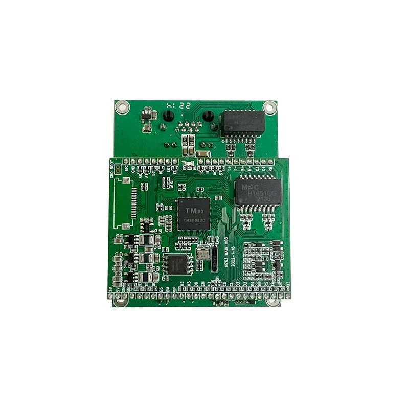
Designing for Manufacturability
Finally, you need to design the RF SIP PCB board with manufacturability in mind. Make sure the design is compatible with the manufacturing processes and equipment. For example, use standard component sizes and footprints so that they can be easily assembled on the PCB.
Also, consider the cost of manufacturing. Try to use cost - effective materials and manufacturing techniques without sacrificing the performance. You can work closely with your manufacturing partner to optimize the design for cost - effective production.
Conclusion
Designing a good RF SIP PCB board is a complex but rewarding process. By following the steps I've outlined above, you can create a high - performance, reliable RF SIP PCB board. Whether you're designing an Intercom Circuit Board or a VoIP board, these principles apply.
If you're in the market for high - quality SIP PCB boards or need some advice on RF SIP PCB design, don't hesitate to reach out. I'm here to help you with all your PCB needs. Let's work together to bring your RF projects to life!
References
- "RF Circuit Design: Theory and Applications" by Chris Bowick
- "Printed Circuit Board Design: Layout and Manufacturing" by Mark I. Montrose
- Various industry - specific whitepapers and technical articles on RF PCB design.