

Signal crosstalk is a common and troublesome issue in the design and manufacturing of SIP PCB boards. As a professional SIP PCB Board supplier, we understand the importance of minimizing signal crosstalk to ensure the reliable performance of electronic devices. In this blog, we will explore various strategies and techniques to reduce signal crosstalk on a SIP PCB board.
Understanding Signal Crosstalk
Before delving into the solutions, it's crucial to understand what signal crosstalk is. Signal crosstalk occurs when a signal from one circuit or transmission line interferes with another nearby circuit or line. This interference can cause noise, distortion, and even data errors in the affected signals. Crosstalk can be classified into two main types: capacitive crosstalk and inductive crosstalk.
Capacitive crosstalk is caused by the coupling of electric fields between adjacent conductors. When a signal on one conductor changes, it creates an electric field that can induce a voltage on a nearby conductor. Inductive crosstalk, on the other hand, is due to the coupling of magnetic fields. As a current flows through a conductor, it generates a magnetic field that can induce a current in a neighboring conductor.
PCB Layout Design
One of the most effective ways to reduce signal crosstalk is through proper PCB layout design. Here are some key considerations:
Trace Spacing
The spacing between traces is a critical factor in minimizing crosstalk. Increasing the distance between adjacent traces reduces the coupling between them. As a general rule, the minimum trace spacing should be at least equal to the trace width. For high - speed signals, even greater spacing may be required. For example, in a high - frequency SIP PCB board, a trace spacing of 0.5 mm or more might be necessary for signals operating at frequencies above 1 GHz.
Layer Stackup
The layer stackup of the PCB can also have a significant impact on crosstalk. Using a multi - layer PCB with dedicated power and ground planes can help isolate signal traces. Signal traces should be routed on different layers with power and ground planes in between. This arrangement provides a low - impedance return path for the signals and reduces the magnetic coupling between traces. For instance, a four - layer PCB with a top signal layer, a ground plane, a power plane, and a bottom signal layer can be an effective configuration for reducing crosstalk.
Differential Pair Routing
Differential pairs are a pair of traces that carry complementary signals. By routing differential pairs closely together and maintaining equal lengths, the effects of crosstalk can be minimized. The differential signals cancel out the common - mode noise caused by crosstalk. When routing differential pairs, it's important to keep the spacing between the two traces consistent and to avoid sharp bends or vias that could introduce impedance mismatches.
Component Placement
Proper component placement can also contribute to reducing signal crosstalk. Here are some guidelines:
Separation of Sensitive Components
Sensitive components, such as high - gain amplifiers or analog - to - digital converters, should be placed away from noisy components, such as switching power supplies or high - speed digital circuits. This physical separation helps prevent crosstalk between sensitive and noisy signals.
Component Orientation
The orientation of components can also affect crosstalk. For example, placing components with long leads parallel to each other can increase the coupling between them. Instead, components should be oriented in a way that minimizes the length of the coupling path between their leads.
Shielding
Shielding is another effective method for reducing signal crosstalk. There are two main types of shielding: electromagnetic shielding and electrostatic shielding.
Electromagnetic Shielding
Electromagnetic shielding involves using a conductive material, such as copper or aluminum, to enclose a circuit or a group of components. The shield acts as a Faraday cage, blocking the magnetic and electric fields from interfering with the enclosed components. In a SIP PCB board, a metal shield can be placed over sensitive components or high - speed signal traces to reduce crosstalk.
Electrostatic Shielding
Electrostatic shielding is used to protect against electrostatic coupling. This can be achieved by using a grounded conductive layer or a shielded cable. For example, a grounded copper layer can be placed between two layers of signal traces to reduce capacitive crosstalk.
Signal Termination
Proper signal termination is essential for reducing crosstalk, especially in high - speed circuits. Termination helps to match the impedance of the transmission line and prevent signal reflections. There are several types of termination techniques, including series termination, parallel termination, and AC termination.
Series Termination
In series termination, a resistor is placed in series with the signal source. The value of the resistor is chosen to match the characteristic impedance of the transmission line minus the output impedance of the source. Series termination helps to dampen the reflections and reduce crosstalk caused by reflected signals.
Parallel Termination
Parallel termination involves connecting a resistor between the signal line and the ground or the power supply. The value of the resistor is chosen to match the characteristic impedance of the transmission line. Parallel termination can effectively absorb the reflected signals and minimize crosstalk.
Grounding and Power Distribution
A proper grounding and power distribution system is crucial for reducing signal crosstalk. Here are some important points:
Grounding
A single - point grounding scheme is often preferred in SIP PCB boards. This means that all the ground connections should be connected to a single point to avoid ground loops. Ground loops can cause crosstalk by introducing unwanted currents and voltage differences between different parts of the circuit.
Power Distribution
The power distribution network should be designed to provide a stable and low - impedance power supply to the components. Decoupling capacitors should be placed close to the power pins of each component to filter out high - frequency noise. This helps to reduce the coupling of power - related noise to the signal traces.
Testing and Verification
Once the SIP PCB board is designed and manufactured, it's important to test and verify the crosstalk performance. There are several testing methods available, including time - domain reflectometry (TDR), network analysis, and signal integrity testing.

Time - Domain Reflectometry (TDR)
TDR is a technique used to measure the impedance of a transmission line and to detect any discontinuities or reflections. By analyzing the TDR waveform, it's possible to identify areas of potential crosstalk and to ensure that the transmission line is properly terminated.
Network Analysis
Network analysis involves measuring the scattering parameters (S - parameters) of the PCB. S - parameters provide information about the transmission and reflection characteristics of the circuit, including crosstalk between different ports.
Signal Integrity Testing
Signal integrity testing is used to evaluate the quality of the signals on the PCB. This includes measuring parameters such as rise time, fall time, jitter, and eye diagram. By analyzing these parameters, it's possible to determine the level of crosstalk and to make any necessary adjustments to the design.
Conclusion
Reducing signal crosstalk on a SIP PCB board is a complex but essential task. By implementing proper PCB layout design, component placement, shielding, signal termination, grounding, and power distribution techniques, and by conducting thorough testing and verification, it's possible to minimize the effects of crosstalk and ensure the reliable performance of the PCB board.
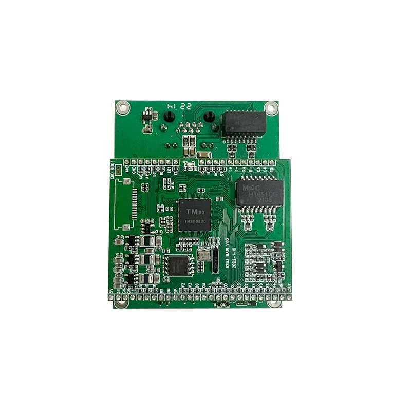
As a leading SIP PCB Board supplier, we have extensive experience in designing and manufacturing high - quality SIP PCB boards with low crosstalk. Our team of experts can work closely with you to understand your specific requirements and to provide customized solutions. If you are interested in our SIP PCB Board, Intercom Board, or VoIP Board, please feel free to contact us for procurement and further discussion.
References
- Johns, D. A., & Martin, K. W. (1997). Analog Integrated Circuit Design. Wiley.
- Montrose, M. I. (2000). Printed Circuit Board Design Techniques for EMC Compliance: A Handbook for Designers. Wiley - Interscience.
- Hall, B. (2009). High - Speed Digital System Design: A Handbook of Interconnect Theory and Design Practices. Wiley.